
X-RAY RUNS: Apply for Beamtime
2017 Nov 1 - Dec 21
2018 Feb 7 - Apr 3
2018 Proposal/BTR deadline: 12/1/17
2018 Apr 11 - Jun 4
2018 Proposal/BTR deadline: 2/1/18
Organic transistors are being hotly investigated for flexible and inexpensive “plastic electronics”applications, such as automobile dashboards and smart tags. A joint team of scientists from the Cornell High Energy Synchrotron Source (CHESS), King Abdullah University of Science and Technology (KAUST) in Saudi Arabia, and Stanford University just reported an experimental break-through for studying the structural evolution of organic transistor layers during the coating process in-situ and in real-time with x-ray scattering. Their paper “Look fast – Crystallization of conjugated molecules during solution shearing probed in-situ and in real time by x-ray scattering“ [1] appeared in the fast publishing journal Physica Status Solidi– Rapid Research Letters and is featured on the cover of the March issue.
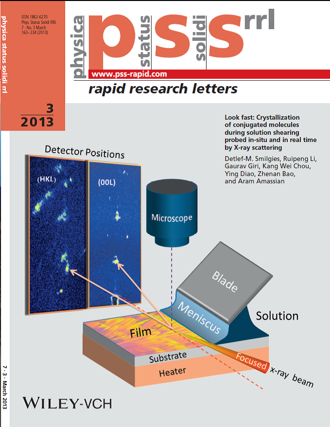
Figure 1. Schematic of the experimental set up to study deposition of organic semiconducting molecules at high spatial and temporal resolution during the coating process. From right to left: x-ray microbeam, precision coating stage displaying a micrograph of a high-quality film, and high-speed x-ray area detector.
The coating procedure pictured on the cover graphics resembles the buttering of a slice of toast turned high tech: The gap between knife and toast needs to be well controlled as well as the speed that the butter is spread. Moreover the toast has to have just the right temperature and the fat content of the butter has to be just so. Leaving the tasty picture, we used a solution of a semiconducting molecule called TIPS pentacene, a silicon wafer kept at a specific temperature for the substrate, and the highly polished edge of a second silicon wafer acting as the knife. The challenge was to devise a precision instrument under the tight space and weight restrictions imposed by the sample goniomenter and the sample microscope. CHESS staff scientist Detlef Smilgies and Gaurav Giri, a graduate student in the Zhenan Bao research group at Stanford University, developed a miniature version of the full-scale coater developed at Stanford.
If the solution is spread too slowly or the temperature too low, a liquid film is spread, and upon drying the same kind of low quality film is obtained, as if the solution had been spread with an eye dropper – the latter techniques is known as drop casting, and obviously much simpler. On the other hand, getting the four critical parameters – gap, speed, temperature, and concentration – just right, the film rapidly thins from the gap value of 100 microns to below 100 nm, i.e. thousand-fold, and then solidifies immediately. All of the action happens under the influence of a viscoelastic shear field. This has the effect that molecular crystallites grow with lateral alignment, despite the fact that the amorphous silicon oxide at the surface of the wafer is isotropic: The shear field breaks the lateral symmetry.
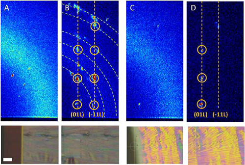
Figure 2. Effect of slow (A, B) and fast solution (C, D) shearing. The top panels show the detector images and the bottom panels the corresponding microscope images; a scale bar of 0.1 mm is shown in panel A. Images mark the beginning (A, C) and the end (B, D) of a solution shearing experiment. Initially only the liquid scattering ring is seen, then crystallization sets in, while the liquid scattering fades. The final film (B, D) is fully crystalline. Strong Bragg reflections (circles) show that at slow speed (A,B), the film has a complex diffraction pattern due to various misaligned crystallites. At optimum speed (C,D) there is only a simple pattern indicating high orientational order of the TIPS-pentacene crystallites. In-situ movies can be obtained free of charge from the Supporting Information [2].
In order to investigate the drying kinetics of the molecules under viscoelastic shear, as the solution meniscus sweeps by, the x-ray beam had to be focused to 20 microns, about half the width of a human hair. With shearing speeds close to 1 mm/sec and a meniscus region of typically 0.5 mm, the time resolution had to be as low as 10 msec per frame, in order to capture the crystallization process. CHESS staff scientist Detlef Smilgies designed the coating stage and the overall experimental set-up employing a high-speed x-ray pixel array detector. Stanford graduate student Gaurav Giri supplied critical coating parameters and helped to develop and test the miniature coater. KAUST postdoc and former CHESS visiting student Ruipeng Li expertly operated the x-ray microbeam and helped to design the overall experiment. The first successful coating experiments are described in the article, and many more data have been taken since by the Stanford team headed by Zhenan Bao and the KAUST team headed by Aram Amassian.
The Stanford team had discovered earlier [3] that films grown with “solution shearing”, as they christened the technique, featured very high mobility, a quality that describes how fast a transistor can switch. Correlated to the high mobility achieved, the molecular structure appeared to be strained, with Bragg reflections moved away from the positions of equilibrium drop-cast films. The CHESS experiments promise to reveal further intricate detail of deposition process and structure formation.
At a first glance solution shearing appears very similar to classic coating techniques used in industrial mass production, known as knife coating or doctor blading. The difference lies in the exquisite control of the coating parameters employed in solution shearing – in classic coating technology typically liquid films are deposited at a specific film thickness while the key to solution shearing is the deposition of solid films at the edge of the meniscus. With careful attention to the deposition parameters, solution shearing will be scalable to large-scale roll-to-roll processing. This capability will be essential for industrial-style production of solar cells, room lighting, and flexible displays based on organic electronics.
This article was also featured in the Cornell Chronicle; (also pdf). A copy or parts of the Chronicle article were posted at Materials Views, Phys Org, and R&D Magazine.
References:
[1] Detlef-M. Smilgies, Ruipeng Li, Gaurav Giri, Kang Wei Chou, Ying Diao, Zhenan Bao, and Aram Amassian: “Look fast – Crystallization of conjugated molecules during solution shearing probed in-situ and in real time by x-ray scattering”, Physica Status Solidi – Rapid Research Letters 7, 177-179 (2013).
[2] Supporting Information: http://onlinelibrary.wiley.com/doi/10.1002/pssr.201206507/suppinfo
[3] Gaurav Giri et al.: “Tuning charge transport in solution-sheared organic semiconductors using lattice strain”, Nature 480, 504- 509 (2011).
Submitted by: Detlef Smilgies, CHESS, Cornell University
4/11/2013