
X-RAY RUNS: Apply for Beamtime
2017 Nov 1 - Dec 21
2018 Feb 7 - Apr 3
2018 Proposal/BTR deadline: 12/1/17
2018 Apr 11 - Jun 4
2018 Proposal/BTR deadline: 2/1/18
K D. Finkelsteina,1, R. Jonesb, A. Paulinga, Z. Browna, A. Tarunc, S. Jupitzd, D C. Sagane, D S. Misrac
aCHESS, Cornell University, bDepartment of Physics, University of Connecticut, cIIa Technologies, Singapore, dSt. Mary’s College of Maryland, eCLASSE Cornell University
The CHESS monochromatic x-ray topography capability was reported on this summer at SRI-2015. The system (shown schematically below), typically available 6 weeks per year based on user demand at station C1, consists of a beam expanding monochromator, 6-circle diffractometer, and CHESS designed CMOS camera with real time sample-alignment capability. Users can collect rocking curve maps with angle resolution as small as 2μradians, spatial resolution to 3 microns, and field of view up to 7mm. The capability has been applied to: improve CVD-diamond growth, evaluate perfection of ultra-thin diamond membranes, correlate performance of diamond electronics to crystal defect structure, and for defect analysis of single crystal silicon carbide.
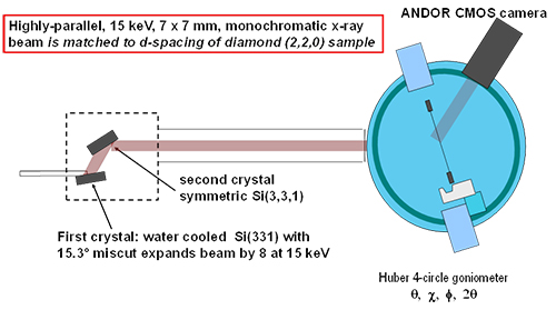
Figure 1: Schematic view of CHESS beamline C1 topography setup. The upstream silicon (331) mono crystal is asymmetric with expansion factor (|b|) of 8 at 15KeV. The second symmetric (331) crystal passes the vertically expanded beam. Beam size at the sample (at the center of a Huber diffractometer), controlled by silts upstream of the mono, can be as large as 7mm x 7mm.
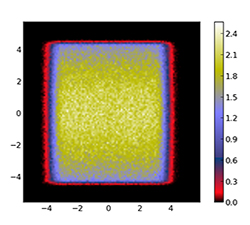
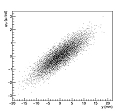
Figure 2: Left: shows simulated intensity distribution at the sample for 1mm(V) by 8mm(H) beam at the mono, done using Bmad[1]. The figure at right shows effective vertical angle distribution ψV = θV - (Δk / k0) tan(θBragg) vs. vertical position y at sample. ΘV, Δk / k0 are respectively beam vertical divergence, and bandwidth emerging from monochrometer. These simulations assume a Gaussian vertical source size 280 microns(RMS), 50 uradian source divergence, distance to silicon (331) mono 10.5 m, expansion factors: b=8 (reflecting up) followed by b=1 (reflecting down), mono-sample distance 4.0 meters, and diamond (220) target reflecting up. Results on right assume slits do not limit incident beam at mono.
Typical Applications
IIa Technologies grows ultra-high purity CVD diamond plate detectors, correlating width histograms from rocking curve maps with measured charge collection efficiency(CCE) and gamma ray energy resolution[2,3]. Samples with broad distribution and high average width have low CCE, while poor energy resolution is correlated with long histogram tails. Lattice disruption is thought to affect drift velocity of holes and electrons reducing detector energy resolution.
Figure 3: Color images are maps of IIa Technologies CVD diamond plate rocking curve angle FWHM. Top images are (220) reflection when plate is rotated by 90˚ about surface normal. The color bar applies to all color maps. Lower images show (400) width and reflectivity. Histograms at right show RMS distribution of rocking curve width extracted from the images.
GlueX[4] experiments at Jefferson Lab measure the spectrum and decays of excited mesons. Probing the dynamics of gluons in the atomic nucleus requires a polarized beam of high energy (≥ 9 GeV) photons. The source of photons is a diamond crystal that emits high-energy polarized light when high-energy electrons pass through by the process of coherent bremsstrahlung. This is similar in many ways to x-ray diffraction but it takes place at orders of magnitude higher energy when the product of incidence angle and photon wavelength matches the atomic scale. At 9 GeV, this requires control of the beam incidence angle at the μradian level. Achieving this degree of alignment requires lattice flatness and strain characterization using high-resolution x-ray diffraction at a facility like CHESS.
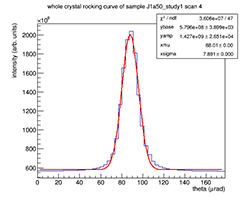
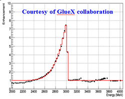
Figure 4: GlueX requires 20 micron thick diamonds with (220) RMS reflection width below 20 μradians at 15KeV. Measured rocking curve (left), from sample 2.5 times thicker than the design goal, has width 7.9μrad RMS, well within experimental requirements. The preliminary photon spectrum (right) is from this sample placed in a 6 GeV Jefferson Lab electron beam during a Spring 2015 commissioning run. Electron beam energy was half the GlueX design energy, but these data provide a first look at performance of the GlueX photon source. Vertical axis is the ratio of photon intensity from the diamond to that of an amorphous radiator of equivalent thickness. Agreement is good between measured (black points) and expected spectral ratio for a perfect diamond (red histogram). This sample was selected from more than a dozen as the best 50 micron target. The goal is to achieve comparable results with thinner diamonds, for operation at 12GeV.
References:
[1] D.C. Sagan, Nuclear Instruments and Methods in Physics Research A, 558, (2006).
[2] J. W. Keister, et al., Nucl. Instrum. Methods Phys. Res. A 649, 91 (2011).
[3] A. Tarun, et al., “Performance of CVD Diamond based Detectors”, Diamond & Related Materials, in press
[4] https://halldweb.jlab.org/wiki/index.php/GlueX_Physics
Submitted by:
Ken Finkelstein, CHESS, Cornell University
11/23/2015