
X-RAY RUNS: Apply for Beamtime
2017 Nov 1 - Dec 21
2018 Feb 7 - Apr 3
2018 Proposal/BTR deadline: 12/1/17
2018 Apr 11 - Jun 4
2018 Proposal/BTR deadline: 2/1/18
The paramount goal of organic electronics is to achieve high mobility in organic transistors within solution-based coating methods that can be scaled up to meet industrial production conditions. Organic field-effect transistors (OFETs) find multiple applications, for instance as switches in active displays, radio frequency identification tags, or flexible biomedical sensors. The mobility of an organic semiconductor film is a measure for the velocity of charge carrier transport and is reflected in the operational speed of the device. Normally, the single crystal of an organic semiconductor achieves higher mobility than a thin film by several orders of magnitude, but would be hard to implement in solution-based production processes. Recently the Amassian group at King Abdullah University of Science and Technology (KAUST) demonstrated that similar mobility can be achieved in organic semiconductor films by knife-coating a solution of a blend of the organic semiconductor with an insulating polymer [1].
Graduate student Muhammad Rizwan Niazi used the soluble organic semiconductor difluoro triethylsilylethynyl anthradithiophene (diF-TES-ADT). He showed that blending diF-TES-ADT with the common polymer polystyrene (PS) yields an improved morphology of the organic film with larger domain size. Using a higher molecular weight, i.e. a PS polymer with longer chain length, produced even better results.
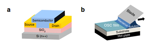
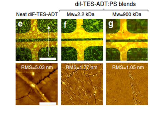
Figure 1: (a) schematic image of a bottom-contact bottom-gate OFET with the organic semiconductor coated on top. (b) schematic image of the knife-coating set-up used (see also [2]). (e-g) Polarized optical microscopy (top row) and AFM (bottom row) images of the coated films. The organic semiconductor appears green, while the gold contacts show as yellow in the microscopy images. The films show increased grain size (top) and reduced roughness (bottom r.m.s. values).
The films with the best performance featured up to 50% polymer content. Cross-sectional electron microscopy revealed the mechanism: the polymer phase separates and preferentially solidifies close to the gate oxide while the organic molecule crystallizes on top of the polymer film. It is not yet fully understood as to why the semiconductor film yielded larger grains with fewer visible grain boundary defects. One key observation was that the surface roughness of the films, as characterized with AFM, decreased by using the higher molecular weight polymer.
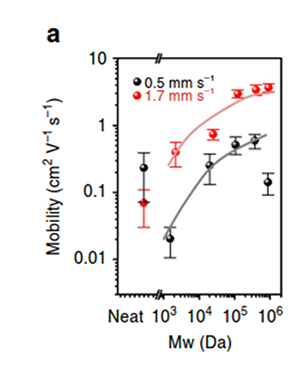
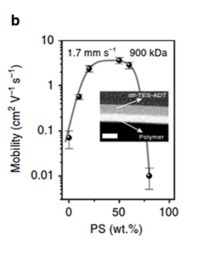
Figure 2: Effect of blending the organic semiconductor with an insulating polymer. Panel (a) shows that the mobility increases with the chain length of the polymer. The effect is even more favorable at higher coating speed. Panel (b) shows that at a polymer content between 25% and 50% by weight the highest mobilities are achieved. The inset shows a cross-sectional electron microscopy image showing the phase separation of the blend into nanoscale polymer and dif-TES-ADT layers.
In a final part of the study the influence of the solvent on growth morphology and performance was studied. Mesitylene and anisole and their mixtures were used as solvents; the highest mobilities of 6.7 cm2/Vs were achieved with an 80%:20% mix of mesitylene and anisole, surpassing the single crystal mobility of 6 cm2/Vs.
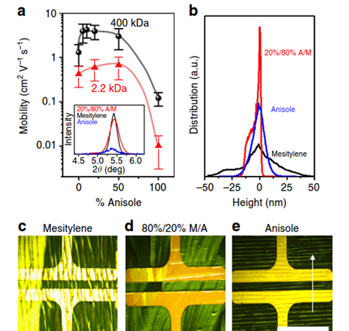
Figure 3: Optimizing the solvent – mesitylene, anisole, and there mixtures were investigated. (a) mobility and (b) roughness as a function of anisole content in the solvent. (c-e) polarized optical microscope images of the coated films. The film coated from the 80%:20% mesitylene anisole mix produces nice flat.
Single crystal mobilities were obtained for the organic semiconductor diF-TES-ADT by fine tuning the blending with a polymer, optimizing coating conditions, and the solvent mixture, while ensuring the semiconductor did not change into a different polymorph. Ex-situ GIWAXS measurements done at CHESS D-line confirmed that diF-TES-ADT crystallized in the same polymorph in the pure material and the blend.
References:
[1] Muhammad R. Niazi, Ruipeng Li, Er Qiang Li, Ahmad R. Kirmani, Maged Abdelsamie, Qingxiao Wang, Wenyang Pan, Marcia M. Payne, John E. Anthony, Detlef-M. Smilgies, Sigurdur T. Thoroddsen, Emmanuel P. Giannelis & Aram Amassian: “Solution-printed organic semiconductor blends exhibiting transport properties on par with single crystals”, Nature Commun. 6:8598 (2016); DOI: 10.1038/ncomms9598
[2] http://news.chess.cornell.edu/articles/2013/Smilgies04112013.html; Detlef-M. Smilgies, Ruipeng Li, Gaurav Giri, Kang Wei Chou, Ying Diao, Zhenan Bao, and Aram Amassian: “Look fast – Crystallization of conjugated molecules during solution shearing probed in-situ and in real time by x-ray scattering”, Physica Status Solidi – Rapid Research Letters 7, 177-179 (2013).
Submitted by: Detlef Smilgies, CHESS, Cornell University and Aram Amassian, KAUST
04/14/2016