
X-RAY RUNS: Apply for Beamtime
2017 Nov 1 - Dec 21
2018 Feb 7 - Apr 3
2018 Proposal/BTR deadline: 12/1/17
2018 Apr 11 - Jun 4
2018 Proposal/BTR deadline: 2/1/18
With continued scaling of nanostructures used in semiconductor devices at sub-10 nm technology nodes, development of new conformal deposition and annealing processes, and testing of their compatibility with high mobility transistor channel materials, such as III-V and Germanium (Ge), are required. Because of the self-limiting reactions, atomic layer deposition (ALD) offers high conformality which is greatly desired as the critical features in these nanostructures are approaching atomic dimensions. The structural characterization of these nanoscale structures and thin films require use of synchrotron sources such as CHESS which could provide orders of magnitude higher brilliance leading to faster, high-quality diffraction experiments usually not available at a laboratory setup.
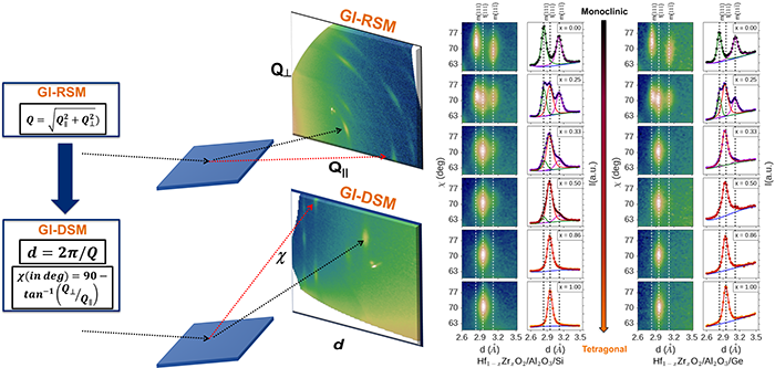 Figure on the left shows conversion of the grazing incidence reciprocal space maps (GI-RSMs) to d-spacing maps (GI-DSMs) for simplicity of indexing, phase identification, and subsequent analysis. The figure on the right shows a particular region of the GI-DSM for the set of films deposited on Al2O3 passivated Ge and Si substrates and determining the phases and amount of ZrO2 content required for the completion of the tetragonal phase formation by automated peak fitting using a script written in python.
In a new article appearing in the Journal of Applied Physics (DOI: 10.1063/1.4963166), researchers working at the experimental facility of Colleges of Nanoscale Science and Engineering, SUNY Polytechnic Institute, have attempted to address this issue by use of a five-step ALD and annealing approach to develop materials that are compatible with Ge and also include controlling the crystal structure via compositional control of ZrO2 into the HfO2 for developing a higher-k dielectric. To elucidate the crystal structure of these higher-k dielectric films of thickness less than 7 nm, the lead author on this work, Dr. Sonal Dey, used grazing incidence reciprocal space mapping technique at the G2 beamline of CHESS. The researchers were able to determine the amount of ZrO2 that is required for complete formation of a tetragonal phase (which is expected to have a higher dielectric constant) in the ALD HfO2 based films, the formation of a Ge rich interfacial layer, and tune the thickness of the Al2O3 passivation layer to suppress the Ge diffusion into the dielectric film stack.
Such thin and ultra-thin structures of dielectric materials with tailored properties are being developed to be used in semiconductor nanostructures which will enable the integrated chip makers with knowledge regarding new integration schemes, processes, and materials for an expanding number of applications requiring increasing computational power. Read the full article here:
SOURCE: S. Dey, et al., Journal of Applied Physics 120 (12), 125304, (2016) DOI: 10.1063/1.4963166; Click here to view the article. http://dx.doi.org/10.1063/1.4963166
Submitted by: Arthur Woll, CHESS, Cornell University
10/04/2016