
X-RAY RUNS: Apply for Beamtime
2017 Nov 1 - Dec 21
2018 Feb 7 - Apr 3
2018 Proposal/BTR deadline: 12/1/17
2018 Apr 11 - Jun 4
2018 Proposal/BTR deadline: 2/1/18
X-ray detectors are an essential part of every x-ray experiment. The most common sensor material for cutting-edge x-ray detection is presently silicon. However, the "stopping power" of silicon is limited; it doesn't efficiently absorb (and ultimately detect) x-rays of energies above approximately 20 keV. For x-ray science applications at higher energies (which are the primary mission of CHESS) different approaches are required; using Cadmium Telluride (CdTe) as a sensor material is one of them. The Gruner group at Cornell has chosen to develop CdTe-based versions of the world-leading MM-PAD and Keck PAD detectors, to allow experiments at x-ray energies up to 200 keV. The results of initial testing at CHESS are reported in a new publication in the Journal of Instrumentation (DOI: 10.1088/1748-0221/11/12/P12013). The tested modules show very few material defects and excellent uniformity in the response to x-rays. Characterization of the CdTe sensors bonded to previously developed electronics show that the material is suitable for use in a broad range of experimental applications. However, an understanding of the (relatively small scale) distortions of the measured signal described in the paper is important in order to understand the limitations of measurements taken with CdTe detectors.
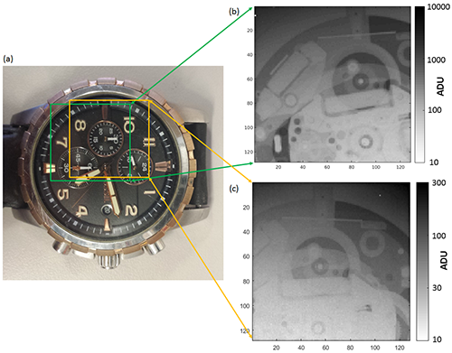 Figure 1: Image (a) and corresponding radiographs of a watch acquired with MM-PAD systems with either CdTe (b) or silicon sensors (c). The image taken with the CdTe sensor was taken in less time, spans a larger range and allows one to discern more detail in the central part of the watch compsared to the image taken with the silicon sensor.
Figure 1 demonstrates the usefulness of the detector as an imaging system. The figure shows a photo of a watch taken by visible light and a radiograph of the same watch with an MM-PAD with a CdTe and a silicon sensor. Since the watch is a macroscopic object containing many thick metal parts, only the high energy part of the x-ray tube illumination will penetrate through it. The figure shows internal features of the watch in higher detail and contrast than seen in the silicon version, despite the CdTe version having been collected in less time. Contrast of the image taken with the silicon sensor is likely also reduced due to Compton scattering (a fundamental scattering process of higher energy photons) within the silicon sensor.
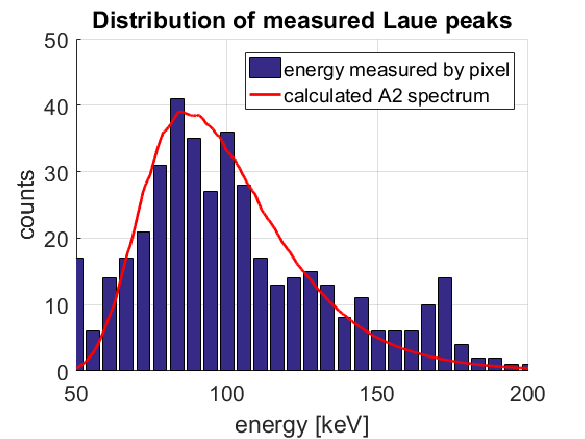 Figure 2: Distribution of the energy determined for each Laue peak. The distribution coincides roughly with the beam spectrum at A2 and diffraction peaks with energies as high as 200 keV have been detected.
The Keck PAD system was used in a white beam experiment at the A2 beamline at CHESS using a Gadolinium-Gallium-Garnet (GGG) crystal as a sample. The energy distribution of the Laue peaks is shown in Figure 2, and compared to the calculated spectrum of the A2 beamline. The figure clearly shows that Laue peaks all the way to the high energy tail of the spectrum at approximately 200 keV were detected. Using this combination of high-flux CHESS beams at CdTe-based fast-framing detectors, dynamic Laue diffraction measurements can be performed with time resolutions in the nanoseconds, an emerging strength for the lab and a new opportunity for exciting future research.
Submitted by: Julian Becker, CHESS, Cornell University
02/06/2017