
X-RAY RUNS: Apply for Beamtime
2017 Nov 1 - Dec 21
2018 Feb 7 - Apr 3
2018 Proposal/BTR deadline: 12/1/17
2018 Apr 11 - Jun 4
2018 Proposal/BTR deadline: 2/1/18
Plastic electronics, in which an organic material replace silicon, has the promise for more cost- and energy-efficient production of mass-produced electronics by avoiding the high vacuum and high temperature processing that characterizes silicon-based devices. However, much remains to be understood about low-temperature solution processing before gadgets using organic circuitry can go into production. The research group of Aram Amassian at King Abdullah University of Science and Technology (KAUST) recently joined forces with Oana Jurchescu’s group at Wake Forest University and of D1 scientist Detlef Smilgies to study the best way to design an organic transistor.
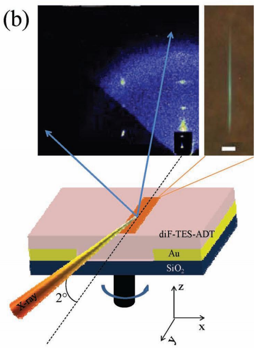
(Fig 1) Scanning microbeam WAXS set-up at CHESS D1 station for device scanning. From bottom to top: x-ray microbeam, organic transistor sample, and x-ray scattering image as recorded on the area detector. The inset shows a micrograph of the microbeam footprint on a fluorescent screen under the same scattering conditions as used for the sample.
The performance of a transistor is usually described by the mobility of the charge carriers – the higher, the better. Effects that adversely impact achieving high mobility are grain boundaries, either between similar molecular crystallites that nucleated at the same time and are misaligned with respect to each other, or crystallites with different growth planes, or even different polymorphs of the material. Interfacial effects play an important role in the texture of the organic layer that crystallizes when the evaporates. Often organic crystallites feature a preferential crystallographic plane parallel to a given substrate. However, a field-effect transistor consists of source and drain electrodes - typically evaporated gold strips - and the gate typically deposited on silicon oxide. Consequently the organic layer may form different growth planes on the different electrode surfaces.
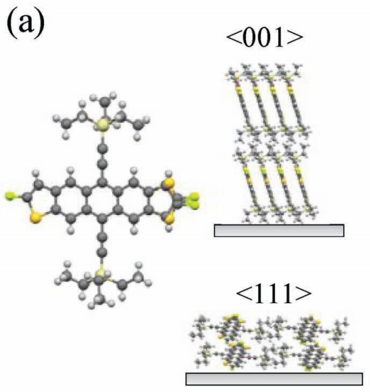
(Fig 2) Thin film morphologies of the semiconducting molecule dif-TES-ADT shown on the left: depending on surface energy the (001) texture or a mix of (001) and (111) textures is assumed.
KAUST postdoc Ruipeng Li and Wake Forest graduate student Jeremy Ward used an x-ray microbeam, in order to probe how the molecular morphology changed when going from source to gate to drain electrode. The microbeam at CHESS D1 station was obtained with an x-ray focusing capillary from the CHESS Capillary Group, and was only 10 microns wide, a fifth of the width of a human hair. This microbeam intercepted the model transistors at a low angle of 2 degrees; the resulting wide-angle scattering revealing the morphology was collected with a CCD camera. They found that the (001) growth plane formed on the gold electrode extended for about 10 microns onto the gate oxide. Then a mix of (001) and (111) planes occurred on the interior of the gate channel. Hence when the gate channel had a width of less than 20 microns, the favorable (001) orientation prevailed, and devices had a good performance, while wider gate channels with mixed morphology performed much more poorly. Next they used a chemical modification of the substrate with a pentafluoro benzene thiol (PFBT) self-assembled monolayer, which made the surface energy differences between electrodes much smaller than for the untreated electrodes. Now the favorable (001)-oriented crystallites covered the device for gate channel widths of up to 50 microns. Their research was recently published in Advanced Materials [1], and is featured on the front cover.
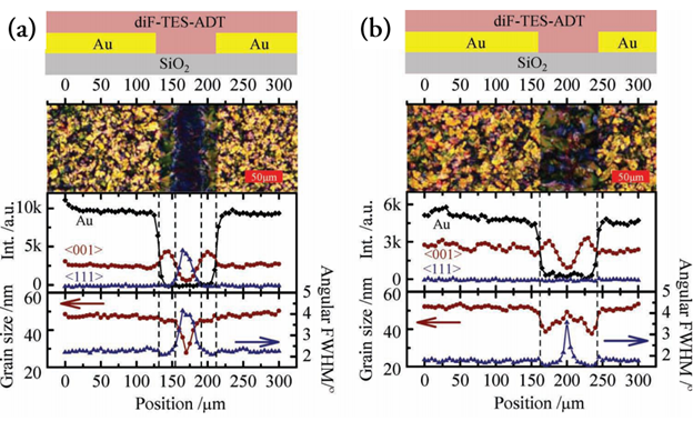
(Fig 3) Cross-polarized micrographs of device channels superimposed with spatially resolved x-ray scattering intensities. Shown are the results for a 50 micron gate channel: (a) for uncoated electrodes the molecular film morphology with preferential (001) growth plane extended about 10 microns from the boundary between gold contacts (source and drain electrodes) onto the silicon oxide layer of the gate electrode. However, in the center of the gate electrode, also the (111) texture was observed and the device had poor performance. When electrodes were coated with a self-assembled monolayer of PFBT the molecular orientation remained (001) resulting in good transistor performance.
Reference:
[1] Ruipeng Li, Jeremy W. Ward, Detlef-M. Smilgies, Marcia M. Payne, John E. Anthony, Oana D. Jurchescu, and Aram Amassian; “Direct Structural Mapping of Organic Field-Effect Transistors Reveals Bottlenecks to Carrier Transport”, Adv. Mater. 24, 5553–5558 (2012)
See article from Wake Forest University: http://www.wfu.edu/academics/physics/news/20/12f-13s/jurchescu/advmater_cover.html
or from the Beacon (Kaust publication): PDF
Also see article from Cornell Chronicle Online: http://www.news.cornell.edu/stories/Nov12/chessOrganic.html; (also PDF)
Submitted by: Detlef Smilgies, CHESS, Cornell University
11/9/2012