
X-RAY RUNS: Apply for Beamtime
2017 Nov 1 - Dec 21
2018 Feb 7 - Apr 3
2018 Proposal/BTR deadline: 12/1/17
2018 Apr 11 - Jun 4
2018 Proposal/BTR deadline: 2/1/18
The production of thin films underlays much of modern technology, from flexible flat screen monitors to future applications of “plastic electronics” in cases such as luminaires, smart tags, and solar energy conversion. While the common process of vacuum deposition of thin film materials onto substrates is well understood, much less is known about how a molecular thin film forms from a liquid solution. This is important because liquid solution methods will enable fast, inexpensive printing of electronics, solar cells and batteries. Because of the liquid medium and the fast evaporating solvent, many traditional surface science tools cannot be applied, with the consequence that it has been difficult to understand and improve printing methods. Aram Amassian at King Abdullah University of Science and Technology (KAUST) and his coworkers from University of Kentucky and CHESS, have now shown that careful measurement of solution concentration and crystallization throughout the drying of the solution allows one to control the way in which the solution to solid phase transformation takes place. This was done by combining quartz crystal monitoring with dissipation (QCM-D) with grazing incidence wide-angle x-ray scattering (GIWAXS) measurements and simple monitoring of the deposited mass.
QCM-D has been extensively used in the biology and bioengineering community to investigate the attachment of proteins to surfaces, such as with biosensors and immunological assays. Amassian and KAUST postdoc Ruipeng Li realized that the QCM-D method would also be a great tool to study the deposition, self-assembly, and crystallization of semiconducting molecules and polymers from the liquid solution phase. In QCM-D two types of metrics are available simultaneously: the frequency shift is related to the amount of material rigidly attaching to the quartz oscillator, while dissipation of mechanical energy during each oscillation relates to the viscoelastic properties of the material interacting with the sensor. By combining these two it is possible to monitor phase transformation from liquid to solid, the rate of film deposition, as well as the presence of residual solvent trapped inside the film.
Time-resolved GIWAXS measurements performed at CHESS D1 station provided a key piece of information: The rate of conversion of solution to solid, which is crucial to growing polycrystalline films conducive to fast charge transport and responsive devices, such as touch screens and other technologies.
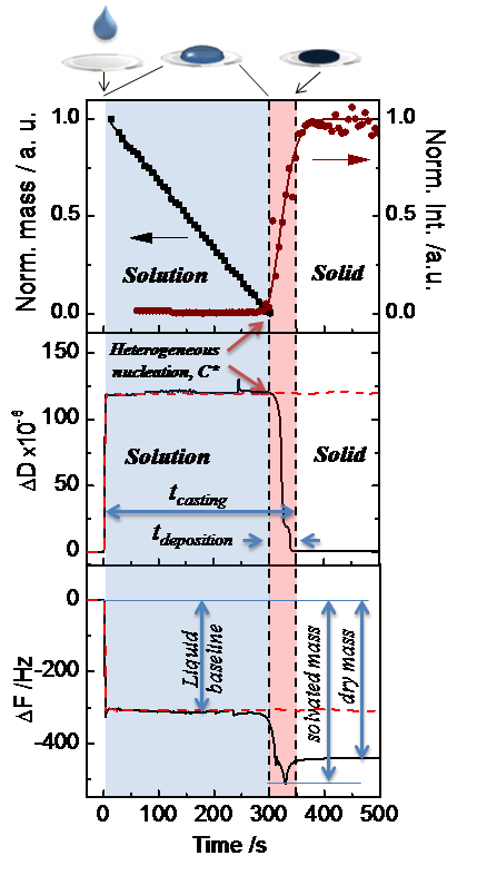
Figure: Top: The normalized change in deposited mass and intensity of the (001) Bragg sheet of TIPS-Pentacene organic semiconductor during a typical drop-casting experiment in ambient conditions. The solid line following the experimental GIWAXS data points corresponds to an Avrami model fit of the crystallization process. Middle: The dissipation shift (ΔD) and Bottom: the frequency shift (ΔF) of the pure solvent drop (dashed red lines) and of the drying TIPS-Pentacene solution (solid black line) in relation to the process time. The process time is initiated (t = 0) upon casting the solution. The key kinetic parameters of drop-casting, including the total casting time (tcasting), the deposition time (tdeposition), the solvated mass (minimum ΔF) and the dry mass (steady state of ΔF), are obtained from the GIWAXS and QCM-D data and yield an estimate of the deposition rate of the film.
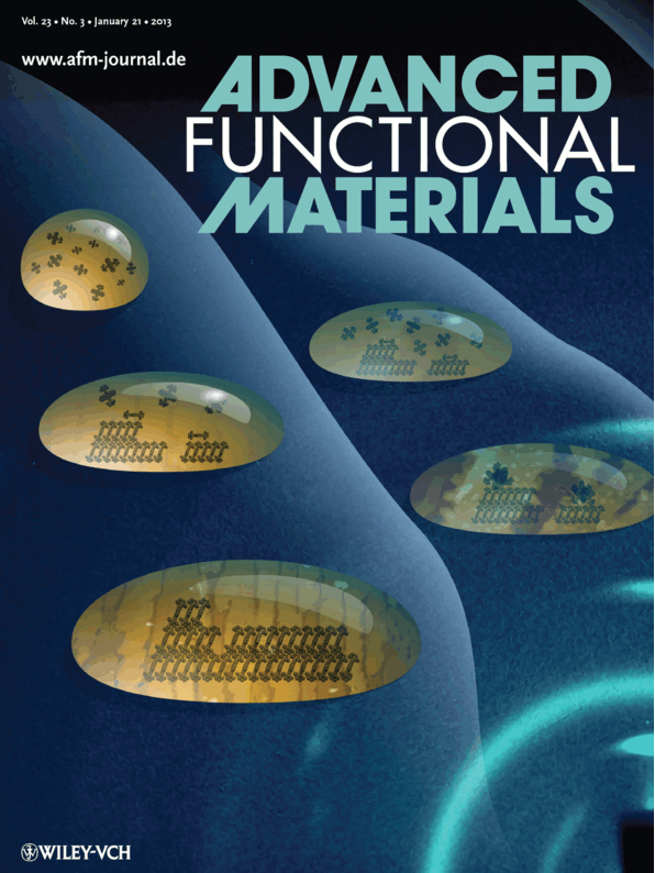
John Anthony and Marcia Payne at the University of Kentucky synthesized and provided the small-molecule semiconductor used in this study. X-ray scattering was performed at D1 station using a solvent vapor cell developed by CHESS staff scientist Detlef Smilgies. A similar chamber was also built at KAUST to enable all the experiments in otherwise identical drying conditions. The results were recently featured on the front cover of Advanced Functional Materials [1].
References:
[1] Ruipeng Li, Hadayat Ullah Khan, Marcia M. Payne, Detlef-M. Smilgies, John E. Anthony, Aram Amassian: “Heterogeneous Nucleation Promotes Carrier Transport in Solution-Processed Organic Field-Effect Transistors”, Adv. Funct. Mater. 23, 291–297 (2013)
http://onlinelibrary.wiley.com/doi/10.1002/adfm.201201264/abstract
Submitted by: Detlef Smilgies, CHESS, Cornell University
1/17/2013