
X-RAY RUNS: Apply for Beamtime
2017 Nov 1 - Dec 21
2018 Feb 7 - Apr 3
2018 Proposal/BTR deadline: 12/1/17
2018 Apr 11 - Jun 4
2018 Proposal/BTR deadline: 2/1/18
For the industrial production of flexible electronics for the consumer market, post-deposition annealing is an important processing step. The purpose of the annealing step is to optimize performance in printed organic circuits. A team of researchers led by Aram Amassian at King Abdullah University of Science and Technology (KAUST) and the Cornell High Energy Synchrotron Source (CHESS) has studied how the improvement of electronic performance is related to the development of microsctructure of the material during solvent annealing [1]. The work is highlighted on the cover of the April issue of ACS Applied Materials and Interfaces, an issue that was dedicated to the development of organic transistor technology.
Figure 1 shows TIPS-pentacene molecules ordering on a flexible substrate under the influence of toluene vapor. Vapor annealing is highly compatible with roll-to-roll processing of organic electronics devices on flexible substrates.
Amassian and colleagues figured out how to tune device performance through control of solvent vapor annealing while depositing organic electronic devices onto a quartz substrate. They in-situ monitored the evolution of morphology, crystalline structure and phase separation during the device fabrication process using novel methods that provided deeper understanding of the post-deposition annealing than tradiational trial-and-error tests. Samples were exposed under varying process conditions and durations and thin film structure and device performance were measured to provide feedback for the device processing. Quartz Crystal Microblanance and Dissipation (QCM-D) measurements were key to providing sensitive quantification of solvent vapor uptake as well as a measure of the mechanical properties of the film in the presence of the adsorbed solvent. QCM-D measures the change of resonance frequency (ΔF) of the quartz crystal onto which the organic device is being deposited. ΔF reports change in mass bound to the surface of the crystal, as well as the energy dissipation (ΔD), which relates to the amount of energy lost per cycle of shear oscillation of the quartz sensor due to changing viscoelastic properties of the bound mass.
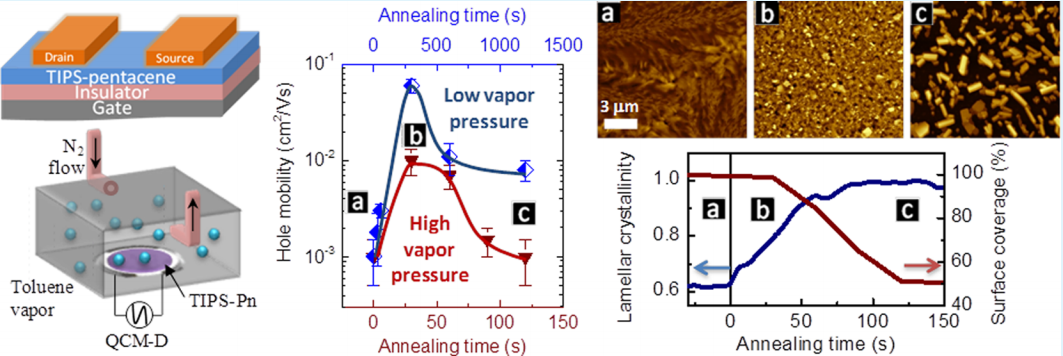
Figure 2. Overview of the KAUST results: A bottom gate transistor (top left) was kept in a closed chamber (bottom left) with a quartz-crystal monitor. A similar chamber could also be used for the x-ray scattering experiments. The middle panel shows the hole mobility as a function of time, as the organic transistor is exposed to toluene vapor at high or low vapor pressure. AFM images taken at various stages of the annealing cycle (a – c and lower rightmost figure) reveal the change in TIPS-pentacene microstructure: over time the material recrystallizes to form larger and larger crystallites. While the recrystallization initially boosted the mobility, extended exposure to vapor led to the formation of large crystallites with holes in the layer, and the mobility decreased again. These results show that proper dosing of the vapor exposure will be essential for the production of organic circuits.
The analysis indicated that the processing occurs in two stages. During the first stage, the film is rigid. The crystalline structure improves, as monitored by in situ X-ray scattering measurement on CHESS D-line, and the transistor mobility increases by up to two orders of magnitude. This suggested that a very small dose of solvent vapor in the molecular regime is capable of dramatically transforming the morphology of the film. With continued exposure to solvent, a second stage follows that includes significant coarsening due to increase of the lateral size of features, but also to formation of a binomial population of flat feature sizes. The observed large isolated crystallites suggested both intra- and inter-grain mass transport and are partly associated to dewetting of the film from the substrate, resulting in low coverage of the substrate and the decay of the mobiliy. The results demonstrate the need of the precise control during solvent vapor annealing, in order to optimize the performance of the organic thin film transistors.
Reference:
[1] Hadayat Ullah Khan, Ruipeng Li, Yi Ren, Long Chen, Marcia M. Payne, Unnat S. Bhansali, Detlef-M. Smilgies, John E. Anthony and Aram Amassian, "Solvent Vapor Annealing in the Molecular Regime Drastically Improves Carrier Transport in Small-Molecule Thin-Film Transistors", ACS Appl. Mater. Interfaces 5, 2325−2330 (2013).
Submitted by: Ruipeng Li and Detlef Smilgies, CHESS, Cornell University
5/28/2013