
X-RAY RUNS: Apply for Beamtime
2017 Nov 1 - Dec 21
2018 Feb 7 - Apr 3
2018 Proposal/BTR deadline: 12/1/17
2018 Apr 11 - Jun 4
2018 Proposal/BTR deadline: 2/1/18
Just out in Journal of Electronic Materials is a novel strain mapping study of crystalline Silicon Carbide, a material widely used as a substrate for thin film electronics. The work was done at CHESS and APS by JIANQIU GUO ,YU YANG, BALAJI RAGHOTHAMACHAR, MICHAEL DUDLEY from SUNY Stony Brook and by CHESS Staff Scientist STAN STOUPIN (before he moved to CHESS).
The group developed a non-destructive method, based on synchrotron double-crystal topography, to quantitatively measure and compare directional components of lattice strain between unprocessed wafers and those subjected to post-growth high-temperature heat treatment. Maps of different strain components are generated from equi-misorientation contour maps as illustrated in Figure 1. This technique is a powerful tool for estimating strain fields, and their analysis shows that normal strain (change in lattice constant along a direction with change in position along that direction) changes much more than do shear/rotation components. This indicates that dilation/compression rather than lattice tilt is the major type of deformation caused by incorporation of nitrogen dopants and nucleation of basal plane dislocations.
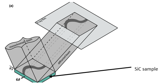 Figure 1: “Equi-misorientation contour” (dark squiggle) results when a crystal is illuminated by a monochromatic, collimated x-ray beam but only a limited region diffracts. When the crystal is rotated by a tiny angle, another region reaches Bragg condition and the contour shifts to a different image position.
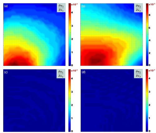 Figure 2: False color strain maps show the magnitude of four different strain components: (a) du1/dx1 (b) du2/dx2 (c) du1/dx3 and (d) du2/dx3.
Submitted by: Ken Finkelstein, CHESS, Cornell University
10/06/2017